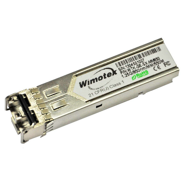
光模块(千兆/双纤/多模550m,850nm/LC)
产品介绍
千兆双纤多模550m,850nm LC接口 3.3v
1. 特征
l SFP package with LC connector
l 850nm VCSEL Laser and PIN photodetector
l Up to 550m transmission on 50/125 um MMF
l +3.3V single power supply
l LVPECL compatible data input/output interface
l Low EMI and excellent ESD protection
l laser safety standard IEC-60825 compliant
l Compatible with RoHS
l Digital Diagnostic SFF-8472 compliant
2. 应用
l Ethernet
l Telecom
l Fiber Channel
3. 极限参数
|
Parameter |
Symbol |
Minimum |
Maximum |
Units |
|
Storage Temperature |
Tst |
-40 |
+85 |
°C |
|
Supply Voltage |
Vcc |
0 |
+3.6 |
V |
|
Operating Relative Humidity |
RH |
5 |
95 |
% |
4. 操作环境
|
Parameter |
Symbol |
Min |
Typical |
Max |
Units |
|
|
Supply Voltage |
Vcc |
3.15 |
3.3 |
3.45 |
V |
|
|
Operating Case Temperature |
Commercial |
Tc |
0 |
|
+70 |
°C |
|
Industrial |
-40 |
|
+85 |
|||
|
Power Dissipation |
|
|
|
1 |
W |
|
|
Data Rate |
|
|
1.25 |
|
Gbps |
|
5. 光学特性
(Ambient Operating Temperature 0°C to +70°C, Vcc =3.3 V)
|
Parameter |
Symbol |
Min. |
Typ. |
Max. |
Units |
|
Transmitter Section |
|||||
|
Center Wavelength |
lo |
840 |
850 |
860 |
nm |
|
Spectral Width(RMS) |
Dl |
- |
- |
0.85 |
nm |
|
Average Output Power |
Po |
-8 |
- |
-3 |
dBm |
|
Extinction Ratio |
Er |
10 |
- |
15 |
dB |
|
Rise/Fall Time(20%~80%) |
Tr/Tf |
|
|
0.26 |
ns |
|
Total jitter |
Tj |
|
|
0.43 |
UI |
|
Optical Eye Diagram |
IEEE 802.3z and ANSI Fibre Channel Compatible |
||||
|
Receiver Section |
|||||
|
Center Wavelength |
lo |
770 |
850 |
860 |
nm |
|
Receiver Sensitivity |
Rsen |
|
|
-19 |
dBm |
|
Receiver Overload |
Rov |
-3 |
|
|
dBm |
|
Return Loss |
|
12 |
|
|
dB |
|
LOS Assert |
LOSA |
-32 |
|
|
dBm |
|
LOS Dessert |
LOSD |
|
|
-19 |
dBm |
|
LOS Hysteresis |
|
0.5 |
|
5 |
|
6. 电学特性
(Ambient Operating Temperature0°C to +70°C, Vcc =3.3 V)
|
Parameter |
Symbol |
Min. |
Typ. |
Max. |
unit |
|
|
Transmitter Section |
||||||
|
Input Differential Impendence
|
Zin |
90 |
100 |
110 |
Ohm |
|
|
Data Input Swing Differential |
Vin |
500 |
|
2400 |
mV |
|
|
TX Disable |
Disable |
|
2.0 |
|
Vcc |
V |
|
Enable |
|
0 |
|
0.8 |
V |
|
|
TX Fault |
Assert |
|
2.0 |
|
Vcc |
V |
|
Deassert |
|
0 |
|
0.8 |
V |
|
|
Receiver Section |
||||||
|
Output differential impendence |
Zout |
|
100 |
|
Ohm |
|
|
Data Input Swing Differential |
Vout |
370 |
|
2000 |
mV |
|
|
Rx_LOS |
Assert |
|
2.0 |
|
Vcc |
V |
|
Deassert |
|
0 |
|
0.8 |
V |
|
7. 脚位说明
|
Pins |
Name |
Discription |
NOTE |
|
1 |
VeeT |
Transmitter Ground |
|
|
2 |
Tx Fault |
Transmitter Fault Indication |
1 |
|
3 |
Tx Disable |
Transmitter Disable |
2 |
|
4 |
MOD DEF2 |
Module Definition 2 |
3 |
|
5 |
MOD DEF1 |
Module Definition 1 |
3 |
|
6 |
MOD DEF0 |
Module Definition 0 |
3 |
|
7 |
Rate Select |
Not Connected |
|
|
8 |
LOS |
Loss of Signal |
4 |
|
9 |
VeeR |
Receiver Ground |
|
|
10 |
VeeR |
Receiver Ground |
|
|
11 |
VeeR |
Receiver Ground |
|
|
12 |
RD- |
Inv. Received Data Output |
5 |
|
13 |
RD+ |
IReceived Data Output |
5 |
|
14 |
VeeR |
Receiver Ground |
|
|
15 |
VccR |
Receiver Power |
|
|
16 |
VccT |
Transmitter Power |
|
|
17 |
VeeT |
Transmitter Ground |
|
|
18 |
TD+ |
Transmit Data Input |
6 |
|
19 |
TD- |
Inv. Transmit Data Input |
6 |
|
20 |
VeeT |
Transmitter Ground |
|
Notes:
1. TX Fault is an open collector output, which should be pulled up with a 4.7k~10kΩ resistor on the host board to a voltage between 2.0V and Vcc+0.3V. Logic 0 indicates normal operation; logic 1 indicates a laser fault of some kind. In the low state, the output will be pulled to less than 0.8V.
2. TX Disable is an input that is used to shut down the transmitter optical output. It is pulled up within the module with a 4.7k~10kΩ resistor. Its states are:
Low (0~0.8V): Transmitter on
(>0.8V, <2.0V): Undefined
High (2.0~3.465V): Transmitter Disabled
Open: Transmitter Disabled
3. MOD-DEF 0,1,2 are the module definition pins. They should be pulled up with a 4.7k~10kΩ resistor on
the host board. The pull-up voltage shall be VccT or VccR.
MOD-DEF 0 is grounded by the module to indicate that the module is present
MOD-DEF 1 is the clock line of two wire serial interface for serial ID
MOD-DEF 2 is the data line of two wire serial interface for serial ID
4. LOS is an open collector output, which should be pulled up with a 4.7k~10kΩ resistor on the host board to a voltage between 2.0V and Vcc+0.3V. Logic 0 indicates normal operation; logic 1 indicates loss of signal. In the low state, the output will be pulled to less than 0.8V.
5. These are the differential receiver output. They are internally AC-coupled 100Ω differential lines which should be terminated with 100Ω (differential) at the user SERDES.
6. These are the differential transmitter inputs. They are AC-coupled, differential lines with 100Ω differential termination inside the module.
8. 电路用途介绍
10. 外形尺寸图